|
| 首页 >> 产品展示 >> 查看产品 |
PCB流程一 |
2014-12-24 14:08:54 |
|
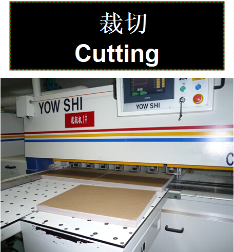
依工单上所指示之发料数和尺寸图,將基板裁切成所需之工作尺寸
Cut according to the quantity and size of working panel listed on the travel card
|


|
修饰裁切后之基板板边,使之平滑,減少板面间及后续制程对涂布轮、底片之刮伤
Edge grind to ensure smooth and reduce scratch by coating tracks and films.
|

|
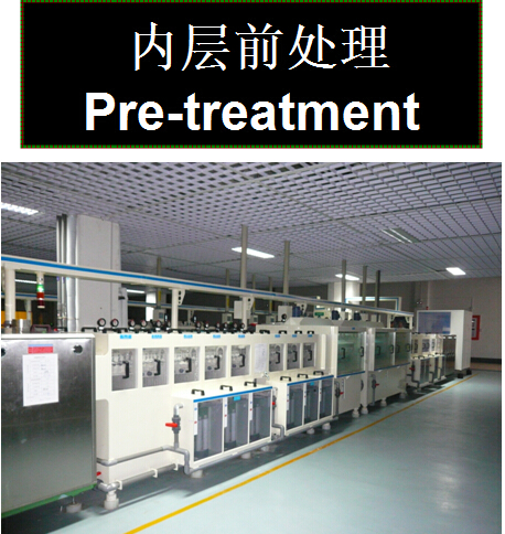
利用药水及磨刷轮与PCB板铜面进行化学/物理反应,达到清洁/粗化铜面目的。
Chemical reactions between brush track and surface of PCB by chemicals to keep clean and coarson the surface.
|

|
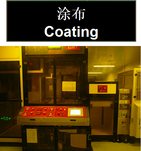
利用滚轮涂布方式在PC板双面垂直覆盖一层感光油墨 Put LPRI on the surface of PCB in vertical direction by track coating.
|

|
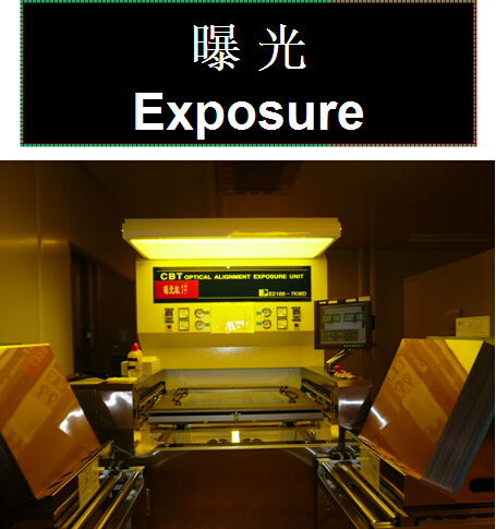
利用紫外线(UV)的能量﹐透过底片照射在板面的感光油墨上﹐使油墨中的光敏物质发生光聚合反应﹐完成影像转移的目的
The PCB with LPRI expose in UV light which penetrates through films to transfer image from film to PCB by photopolymerization.
|

|
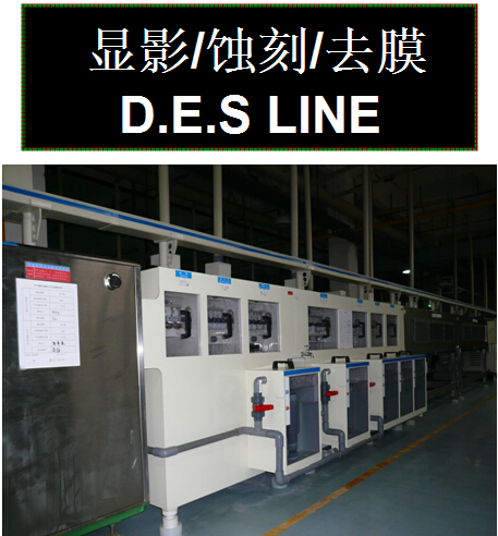
將未受光区域及其膜下之铜层分別用显影液及蚀刻液去除,最后再用去膜液將感光抗蚀层剥除,形成之內层线路图像.
Remove the copper in unexposure area and under film by developing solution and etching solution. And then strip the photosensitive corrosion resistant layer by solution to pattern in inner layer.
|

|
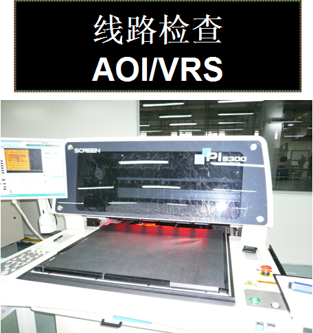
利用CCD镜头抓取投射在板面上”反射光图像”原理﹐对蚀刻后的板面進行扫描﹐并与CAM图像对比﹐进行断路﹑短路﹑残铜﹑缺口等不良点的判读 Implement AOI inspection comparing with CAM data by CCD to avoid open/short/coppper residue/nick defect and so on.
|

|
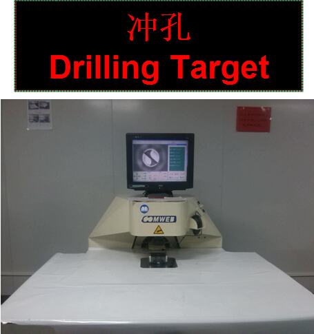
利用CCD抓取靶標中心,配合Spindle对靶标进行中心貫穿作业。Get the target centre by CCD and run through the PCB by spindle.
| |
|
| |
|
|