|
| 首页 >> 产品展示 >> 查看产品 |
PCB流程三 |
2014-12-24 11:33:44 |

|
修饰成型后之板边,使之平滑,減少板面间刮伤
Edge grind to ensure smooth and reduce scratch between working panels. |

|
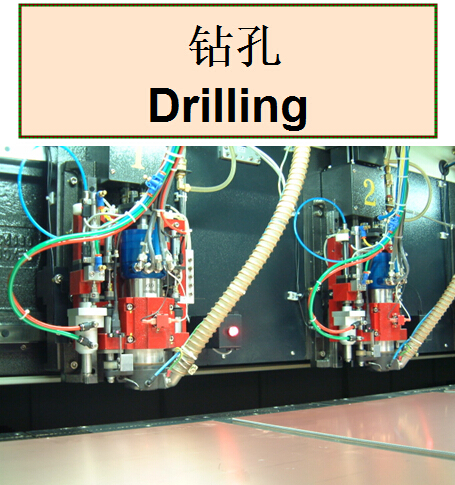
完成导通孔及非导通孔钻孔作业。
Finished drilling the "PTH"and "NPTH"on the single-side.
|


|
利用磨刷及高压水洗,去除钻孔产生的披锋以及粉屑。
Clear away burrs and dust by brusher and water rinse.
|
|
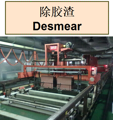
利用化学药水软化并最终去除因钻针高速旋转摩擦孔壁树脂所产生的胶渣,确保内外层能正常导通。
Remove the resin smear caused by high speed drilling in holes by chemical reaction to connect inner layer and outer layer.
|


|
非金属之孔壁沉积一层薄铜,使孔壁金属化﹐使上下铜层与內层铜相连通提供导电性 Deposit a thin copper in hole wall to connect the up and down copper with inner copper for conductivity.
|

|
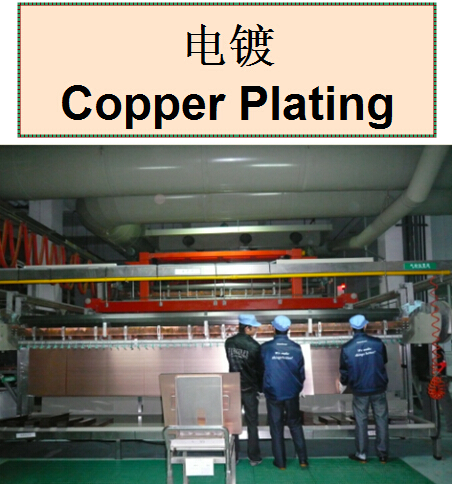
利用电化学原因将铜离子还原成铜金属,使板面及孔内得到我们所需要的镀层厚度
Revert cupric ion to copper metal by electric chemical,which is to get the copper thickness on surface and hole we required.
|

|
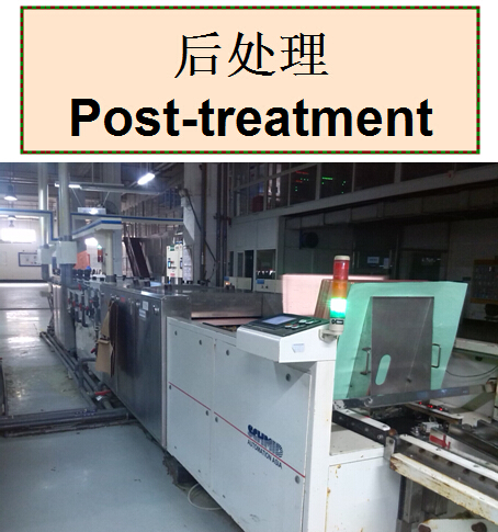
清洁板面氧化物,烘干板面防止氧化。
Clean away the oxidization on the board and dry the board surface to aviod oxidation.
|

|
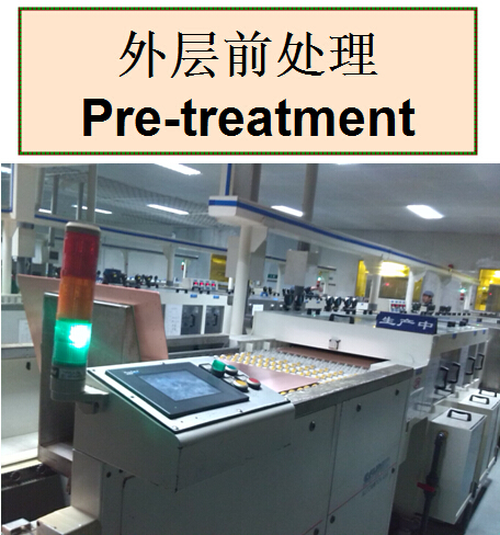
利用磨刷轮对板面進行处理以达到清洁及粗化板面之效果
Clean and coarsen the surface of board by brush track.
|

|
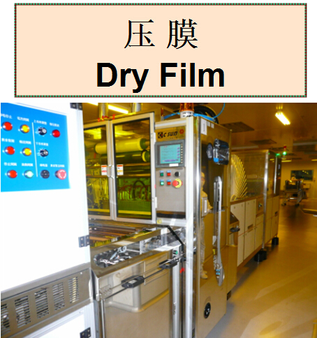
将用于外层线路影像转移基础的半固化干膜通过加热加压,使其紧密贴附于电镀后的板面;
Attach the dry film to the surface of board after plating in high temperature. |


|
利用紫外线(UV)的能量﹐透过底片照射在板面的感光膜上﹐使感光膜中的光敏物质发生光化学反应﹐完成影像转移的目的
The PCB with dry film expose in UV light which penetrates through films to transfer image from film to PCB by photopolymerization. |

|
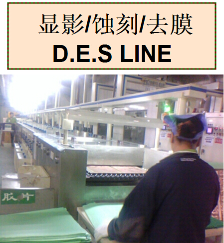
分别用显影液及蚀刻液去除非线路、未感光的干膜及铜层,留下有感光干膜保护的线路,最后去除线路上的干膜,使外层线路显现;.Remove extra dry film and the copper and keep the pattern protected by dry film stay. Then show the pattern of outer layer by stripping dry film.photosensitive corrosion resistant layer by solution to pattern in outer layer. |
|
|
| |
|
|